


The future of advanced manufacturing in the U.S. is being built at innovative facilities that enable experimentation in process and product development. The people and organizations at these next-generation facilities are part of a collaborative effort to remove barriers of entry and create an ecosystem to build supply chains and provide a path for the commercialization of emerging technologies.
These next-generation facilities are working on initiatives that include:
- Using advanced fiber technology to make programmable backpacks that have no wires or batteries but connect to the digital world.
- Using light instead of electronics to power cloud-based data centers, increasing the speed of transfer tenfold while drastically reducing energy use and cost.
- Extending the range of electric vehicles by reducing weight and mitigating energy loss during transfers.
This would not be possible without Manufacturing USA, a network of 16 manufacturing innovation institutes and their sponsoring federal agencies — the Departments of Commerce, Defense and Energy. Manufacturing USA was created in 2014 to secure U.S. global leadership in advanced manufacturing by connecting people, ideas, and technology.
Here’s a look at a handful of next-generation facilities supported by the institutes that are shaping the future of U.S. advanced manufacturing.
PowerAmerica’s X-Fab Silicon Carbide Foundry
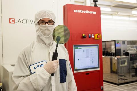
- Location: Lubbock, Texas
- Institute: PowerAmerica
- Sponsor: Department of Energy
- Founding partner: X-Fab Silicon Foundries, a global semiconductor manufacturer
PowerAmerica and X-Fab partnered in 2016 to create the world’s first open silicon carbide foundry, converting a former Texas Instruments facility that made traditional silicon wafers. PowerAmerica’s goal was to remove barriers of entry and help commercialize wide bandgap (WBG) power electronics technologies, which increase the energy efficiency and reliability of power electronics.
Wide bandgap technologies, including both silicon-carbide and gallium-nitride power semiconductors, have implications for legacy power electronics applications such as industrial motor systems, consumer electronics and data systems. More importantly, WBG technologies have proven to meet the needs of next-generation high-voltage applications such as grid modernization, manufacturing plant power systems, off-shore wind, and multi-megawatt motor drives.
The X-Fab foundry operates under a collaborative model, providing companies that lack their own silicon carbide fabrication capabilities with access to a shared production and R&D facility. There are 15 to 20 American companies using the production equipment at various times — some are established companies doing proprietary work and others are startups and smaller companies without their own high volume device production capacity.
AIM Photonics’ Test, Assembly and Packaging Facility
- Location: Rochester, N.Y.
- Institute: American Institute for Manufacturing Integrated Photonics
- Sponsor: Department of Defense
Integrated photonics involve using light for applications traditionally addressed through electronics. It is increasingly being applied in communications, laser-based radar and sensing because it dramatically improves on the performance and reliability of electronic integrated circuits while significantly reducing size, weight, and power consumption.
The AIM Photonics facility is the world’s first open-access Photonic Integrated Chip (PIC) Test, Assembly and Packaging Facility (TAP), making it a key component in AIM’s PIC manufacturing ecosystem by providing a connection point to the photonics supply chain. The TAP facility provides development and production process capabilities that have enabled more than 120 small and medium-sized businesses — which would otherwise be priced out of the market — to bring integrated photonic chip technologies through the product development cycle.
One application being advanced at the facility is photonic sensors using light as radar — or LIDAR. Tiny LIDAR sensors that provide real-time 3D mapping for driverless cars can also be used to manage database systems for cloud computing, detect sarin gases in national security environments, enhance medical imaging and rate food safety by measuring the interactivity of chemicals. Compared to traditional electronics, this new technology can increase data throughput at least tenfold while reducing energy consumption dramatically.
LIFT’s High Bay Facility
- Location: Detroit, Mich.
- Institute: LIFT, which is operated by the American Lightweight Materials Manufacturing Innovation Institute
- Sponsor: Department of Defense
The 100,000-square-foot LIFT High Bay facility opened in 2015 to help private sector members develop, optimize and commercialize their innovations in metrology and lightweight materials manufacturing.
Lightweight, stronger materials continue to be in high demand across aerospace, automotive, and defense industries to increase fuel economy and reduce emissions while using less material and fewer components. The facility has helped people develop transformative processes in melt processing, powder processing, thermo-mechanical processing, novel/agile processing, coatings, and joining and assembly — as well as Integrated Computational Materials Engineering.
High Bay is considered the nation’s premier lightweighting applied research and development facility. It includes:
- Applied research and development space, featuring more than $50 million worth of advanced manufacturing equipment.
- Learning Lab, an immersive space featuring seven unique labs to prepare students for careers in advanced manufacturing through more than 40 workforce initiatives.
- Fast Forge, a technology accelerator to help companies commercialize their technological breakthroughs.
AFFOA’s Fabric Discovery Center
- Location: Cambridge, Mass.
- Institute: Advanced Functional Fabrics of America (AFFOA)
- Sponsor: Department of Defense
The AFFOA Fabric Discovery Center is leading the transformation of traditional fibers, yarns and textiles into highly sophisticated integrated and networked systems. It’s facilitating the conversion of the textile industry into a value-added, high-tech industry, developing innovations such as:
- Programmable backpacks that have no wires or batteries but connect to the digital world.
- An advanced fabric-based hat that receives data from overhead light sources for long distance, directional and high-bandwidth communications.
- Electrophoretic color change, which allows military camouflage to change with locations and environments.
The facility is the world’s first to feature end-to-end prototyping capability, from CAD design to machine tooling to pre-form fabrication and systems integration. It is the nexus of fiber technology all under the same roof — knitting and weaving machines sit next to draw towers, and electrical engineers are close by working on semiconductor device fibers.
Members come to the facility for ideation, development of product concepts, experimentation with processes and consultation with experts and researchers. AFFOA has created the Fabric Innovation Network, which provides access to expertise from all over the country.
BioFabUSA’s Tissue Foundry
- Location: Manchester, N.H.
- Institute: Advanced Regenerative Manufacturing Institute (ARMI)
- Sponsor: Department of Defense
BioFabUSA was established by ARMI to develop an ecosystem for large-scale manufacturing in the emerging sector known as Tissue-Engineering and Regenerative Medicine, which offers the potential for life-changing medical treatments. The tissue foundry is the first demonstration of scalable, modular, automated and closed manufacturing for a tissue-engineered product.
More than 150 members have participated in the tissue foundry, which is composed of a series of manufacturing modules, or subsystems, that begin with the culture of cells and extend to the packaging of a final product. The facility integrates innovative cell and tissue cultures with advances in biofabrication, automation, robotics, and analytical technologies to create disruptive research and development tools and FDA-compliant volume manufacturing processes.
The goal of the Tissue Engineered Medical Products (TEMP) manufacturing process is to produce an automated closed system that is sealed off from the environment, unlike traditional manufacturing. Such a system would not be reliant on costly capital investments in clean room facilities and improve the possibilities of cost-effective operations at scale. Advances in TEMP manufacturing processes will be used to fabricate 3D implants, scaffolds, and tissue constructs.
Larger Initiative Advancing U.S. Manufacturing
These advanced manufacturing facilities are just a few concrete examples of the large-scale support for manufacturing innovation that the Manufacturing USA network of 16 institutes and their sponsoring federal agencies are providing to the U.S. manufacturing sector. Last year the institutes leveraged $133M in federal funds to attract $355M in state and private investment, worked with 1,900 member organizations to collaborate on over 560 major research and development projects. Manufacturing USA institutes partnered with educational organizations to teach thousands of people about advanced manufacturing technologies via workshops, courses, internships, and apprenticeships.
This emphasis is so important because advanced manufacturing increasingly plays a critical role in the U.S. innovation ecosystem, supporting U.S. technological competitiveness and driving product and process improvements that advance the U.S. economy.
To learn more about the work the Manufacturing USA institutes are doing to accelerate advanced manufacturing technologies, visit the institutes page.